Research highlights and themes we are currently pursuing.
Ultrafast melting of ordered phases
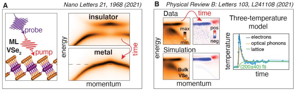
When cooled down below a critical temperature, some metallic 2D materials transform their structures and become more resistive. Such materials hold a promise for realizing ultrafast electronic memory devices, as they can be switched from the insulating to metallic phase upon applying external electric fields. The type of interaction underpinning the ordered phase determines the time it takes for the switching.
In its bulk form, metallic VSe2 undergoes a periodic lattice distortion when cooled down to 110 K. When thinned down to a single layer, the transition temperature is substantially enhanced, and an additional metal-to-insulator transition emerges. We used intense femtosecond laser pulses to bring the two compounds out of their respective ordered phases, and tracked the evolution of their electronic structures by time- and angle-resolved photoemission spectroscopy.
Twisted bilayer graphene
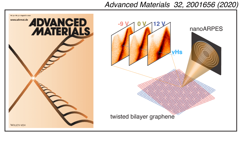
The discovery of correlated behaviour in bilayers of graphene, stacked with an interlayer rotation angle around 1.1 degrees, has triggered an intense effort to understand how this behaviour emerges. Such twisted bilayer graphene (TBLG) exhibits a phase diagram that resembles that of the high temperature cuprate superconductors.
We have investigated the doping dependence of the van Hove singularity in large-angle TBLG devices using nanoARPES, and observe how the hybridised part of the band structure can be shifted near the Fermi level. Further studies closer to the magic angle could provide information on E(k)-resolved many-body excitations in this system.

In-operando nanoARPES
New technical developments in methods to focus X-rays to the nanoscale while collecting angle-resolved photoemission spectra (nanoARPES) are enabling studies of much more complex samples, including functional devices incorporating 2D materials.
We have demonstrated that the dispersion of the Dirac cone in graphene on hBN can be collected using nanoARPES while running a high current density through this stack, as seen in panel A. This data provides the spatially-resolved potential, doping and electron-defect scattering, which can be converted into a map of the local mobility of the graphene device. By supporting such a stack on a graphite back-gate we have also demonstrated that the charge carrier density in the graphene can be varied, while collecting high quality snapshots of the Dirac cone, as seen in panel B. This facilitates a detailed analysis of doping-dependent many-body effects, arising from electron-electron interactions in graphene.
Electronic structure of heterobilayers
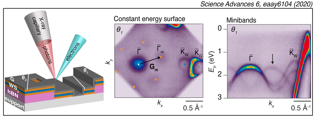
Vertical stacking and twisting of dissimilar 2D materials lead to interesting new quantum states as a result of interactions between the materials. In particular, the superposition of the atomic lattices in the stack establishes a new superlattice, or moiré, with new electronic bands referred to as minibands.
We have used an X-ray capillary in order to micro-focus a synchrotron beam and thereby collect the electronic structure of stacks with variable twist angle between graphene and single-layer WS2. This directly revealed the E(k)-dispersion of minibands at optimum twist angles.
Many-body effects in semiconducting TMDCs
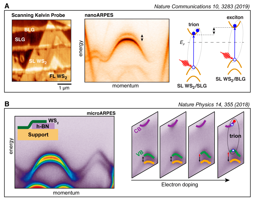
In single layers of transition metal dichalcogenides (TMDCs) such as WS2, electronic screening can be strongly reduced compared to the bulk. This leads to the formation of tightly bound electron-hole pairs, so-called excitons.
Using angle-resolved photoemission with a microscopic (microARPES) or nanoscopic (nanoARPES) synchrotron beam we have probed how different substrates and doping affect these many-body interactions by measuring the energy and momentum resolved spectral function. By synthesising WS2 on alternating stripes of single-layer graphene (SLG) and bilayer graphene (BLG) we observed a rigid band shift in the WS2, following the workfunction change of the underlying SLG and BLG stripes. This leads to a patterned doping effect in the WS2 that locally affects the formation of excitons and charged excitons (trions) as seen in panel A. At extreme doping levels, such trions were observed to dramatically change the splitting of the valence bands in WS2 transferred on a hexagonal boron nitride (hBN) flake, which we tracked in situ during electron doping as seen in panel B.
