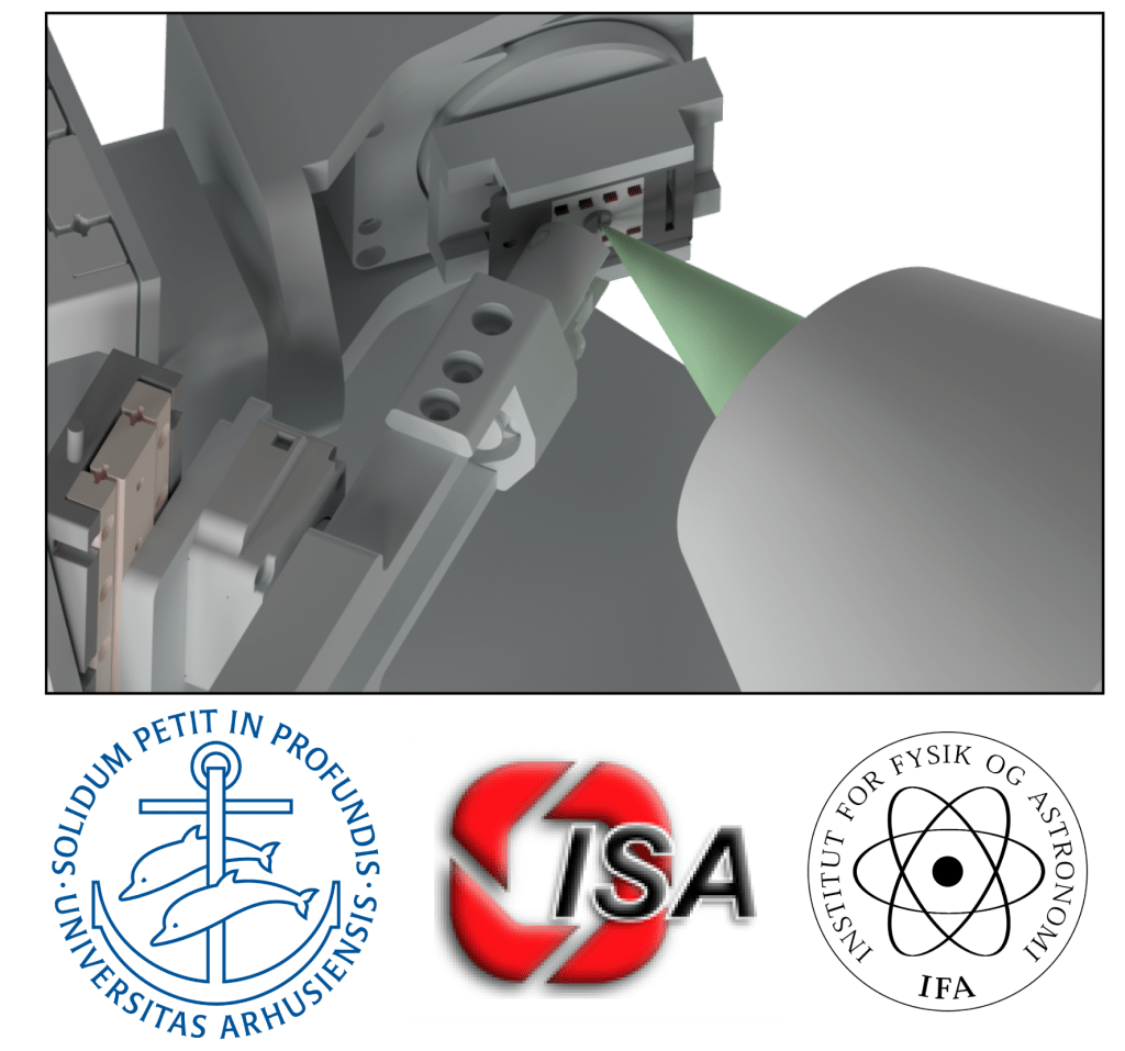
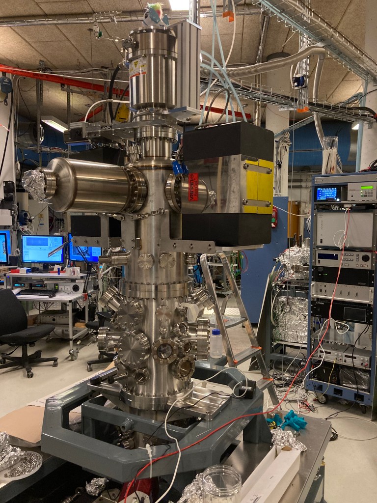
The miniaturisation of electronic devices and the emergence of materials with interfaces at the nano- and micro-meter length scales are calling for new approaches to study the electronic properties of these increasingly complex systems. We have installed a new beamline at the ASTRID2 synchrotron light source in Aarhus, Denmark, which provides access to the electronic structure of such materials by employing angle-resolved photoemission spectroscopy with a submicron light spot (nanoARPES). See a rendering of the experiment to the left.
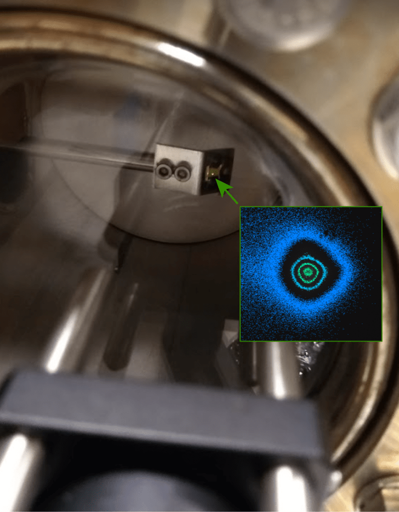
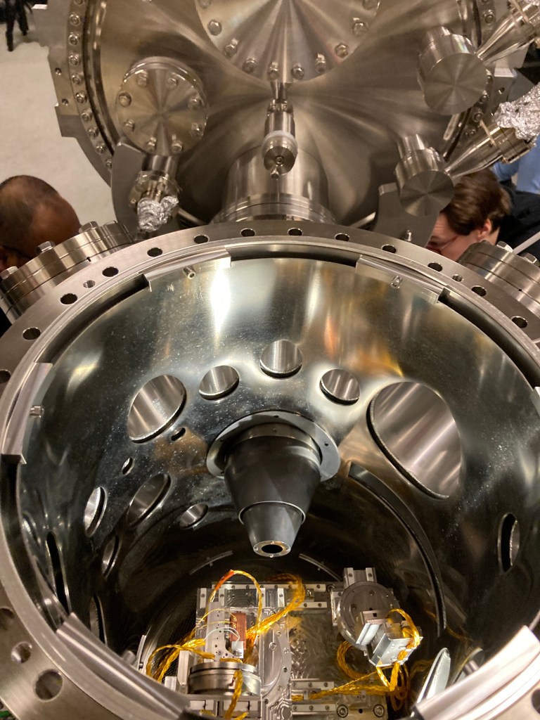
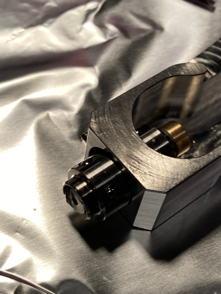
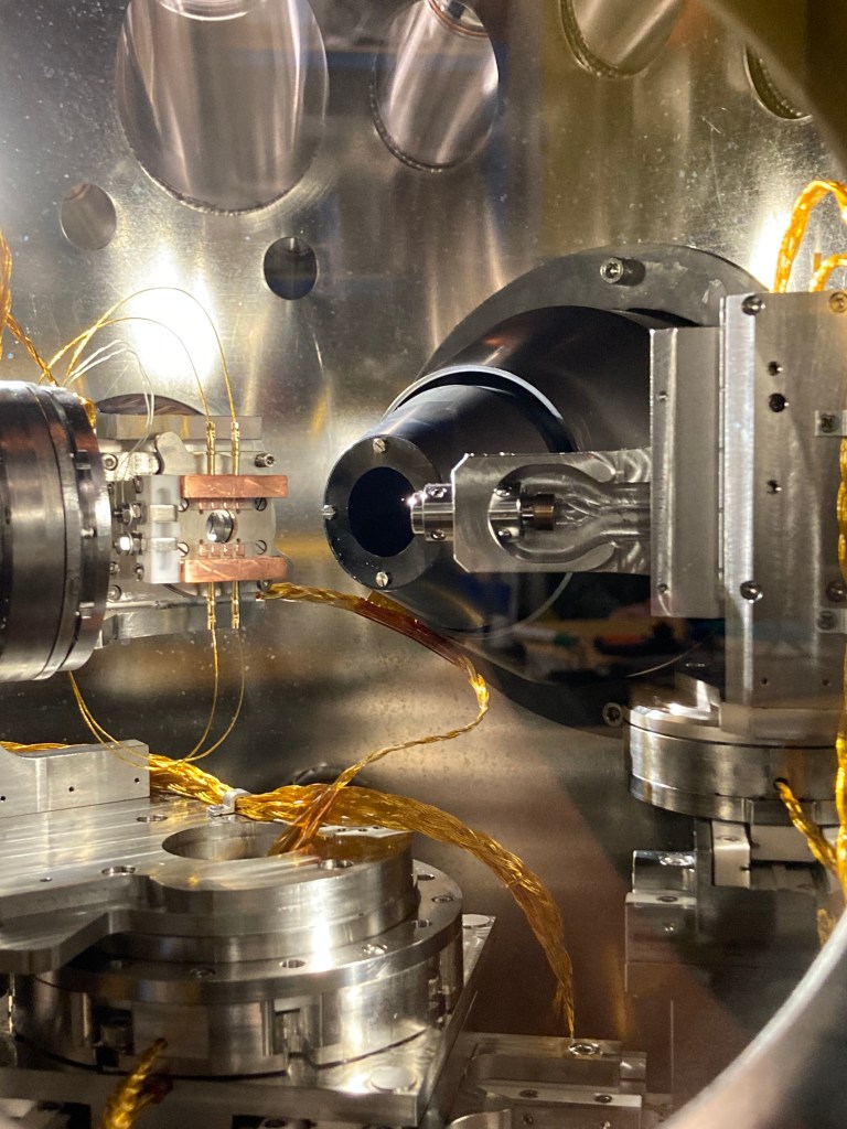
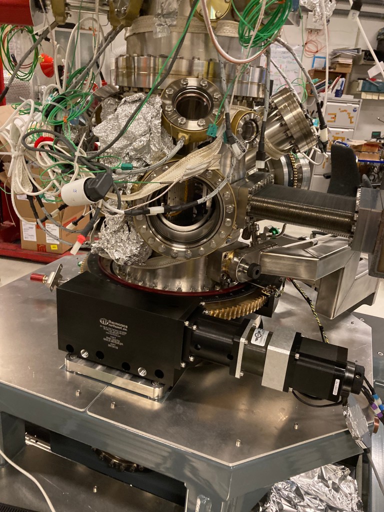
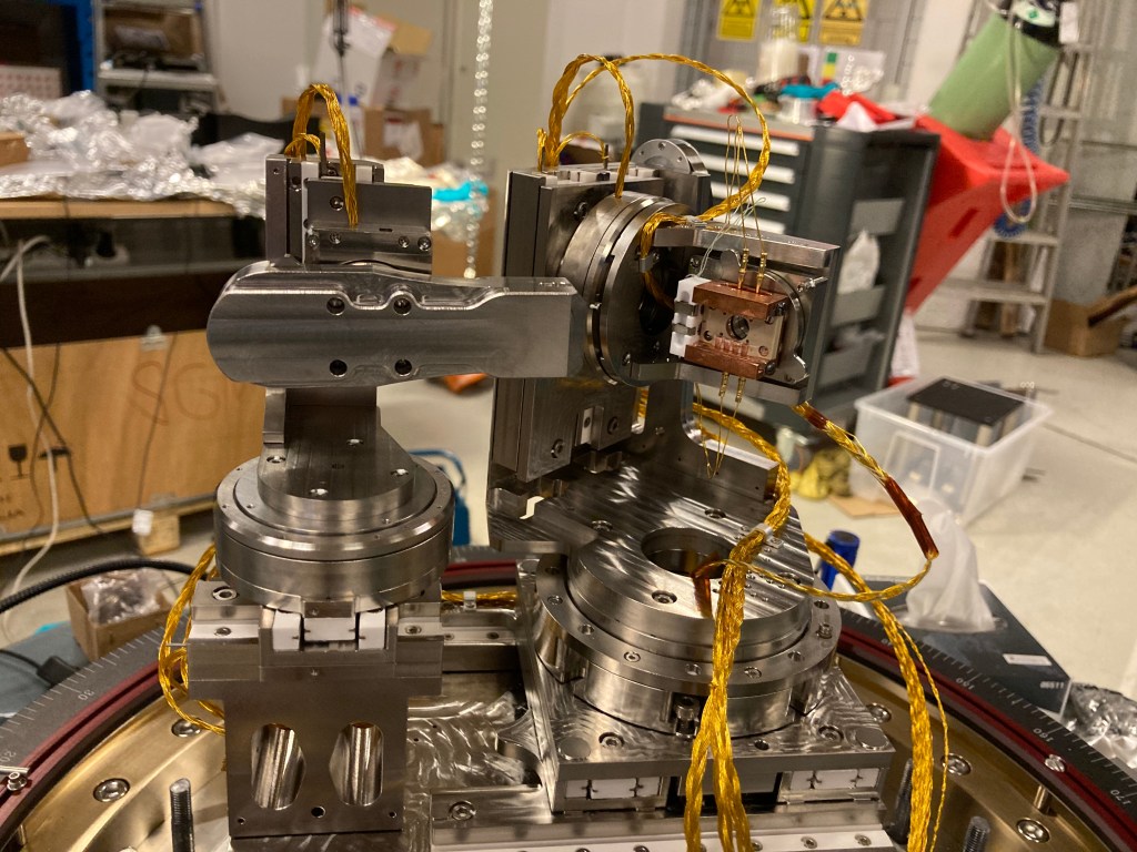
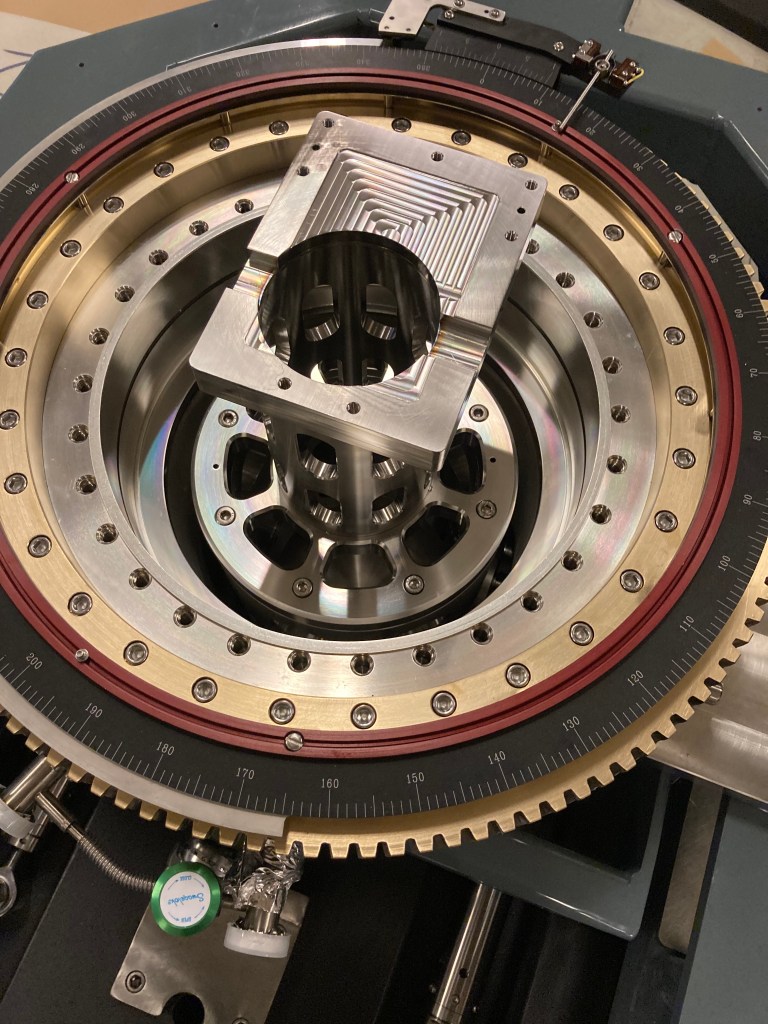
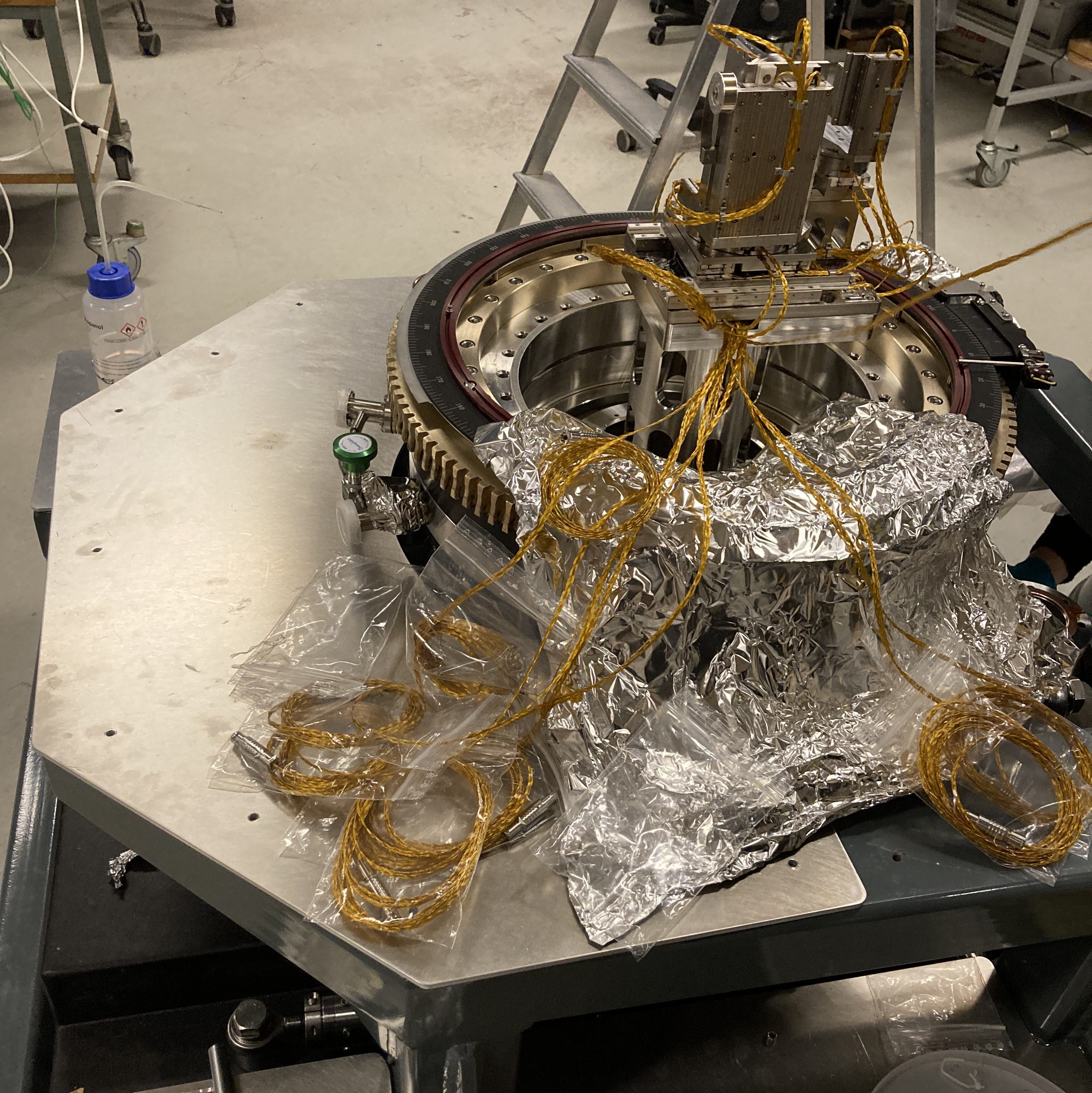
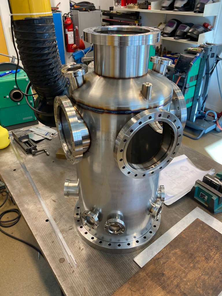
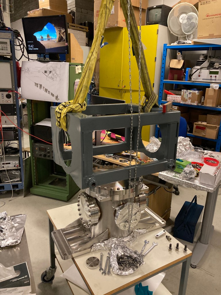
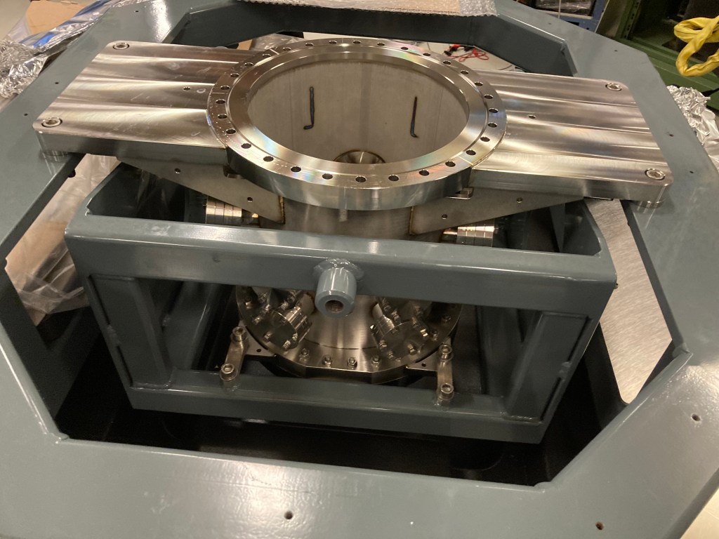
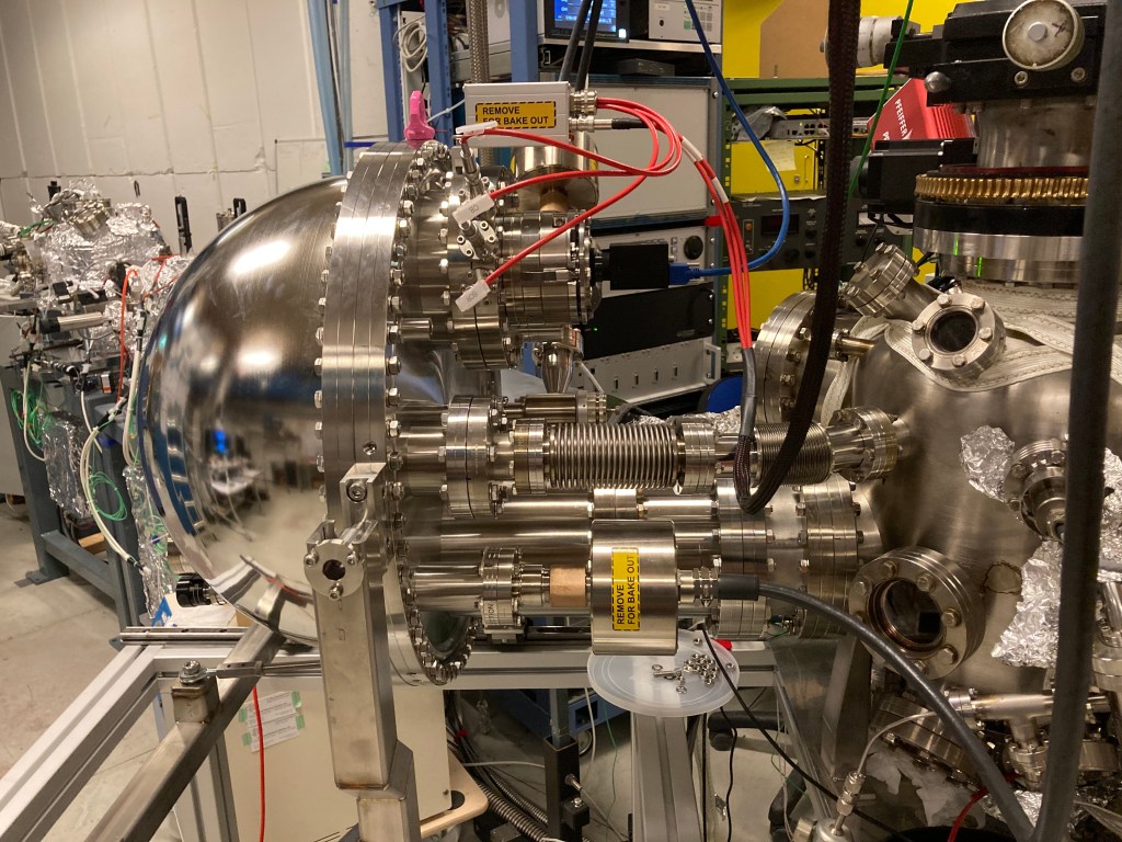
The small focus is achieved using an achromatic capillary, which simultaneously provides a high photon flux and preservers the photon energy tunability of the beamline. Our ultra-high vacuum (UHV) end-station contains a deflection-based hemispherical electron analyzer and an internal microscope stage that incorporates piezo-based motion control with 11-degrees of freedom in order to position the capillary and sample while allowing for cryogenic cooling of samples and electrically contacting devices.
The major new science opportunities enabled by this facility include in-operando spectroscopy of functional devices and probing fundamental interactions in atomically thin custom-made quantum materials. The system will generally enable photoemission from samples with very small feature sizes, on the nano- and microscopic length scales.
The laboratory has recently been expanded with 2D material fabrication setups for building heterostructures and devices.
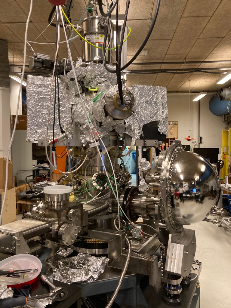
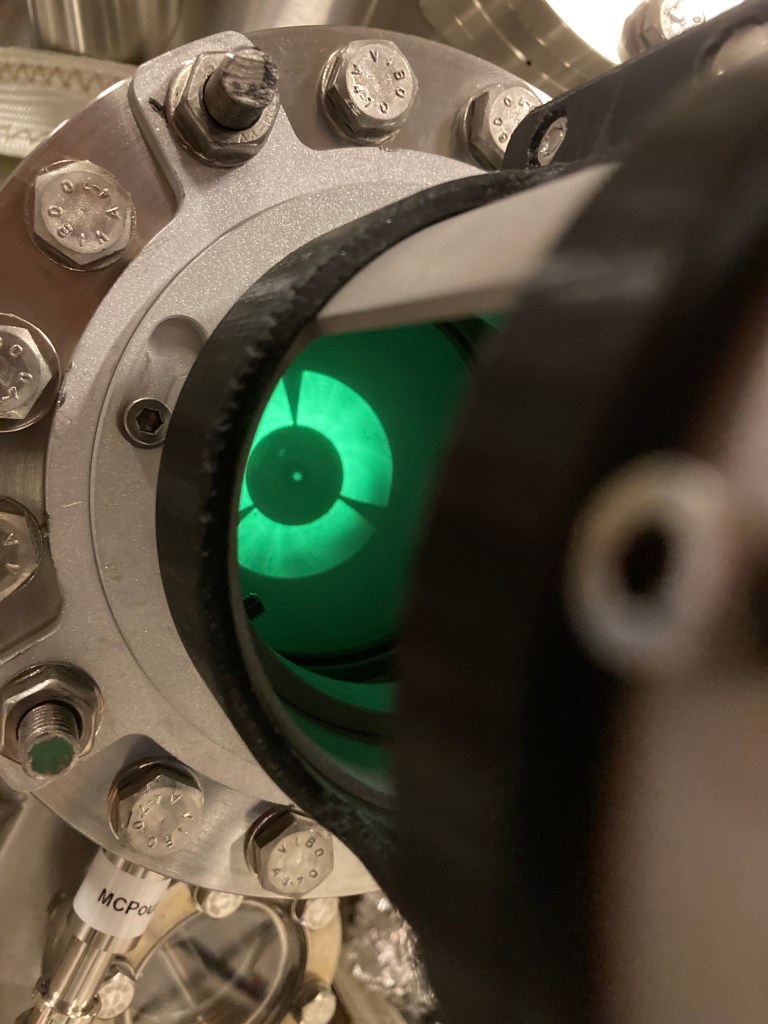
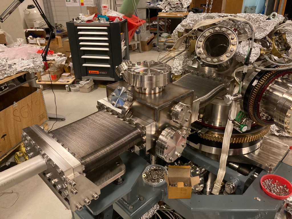
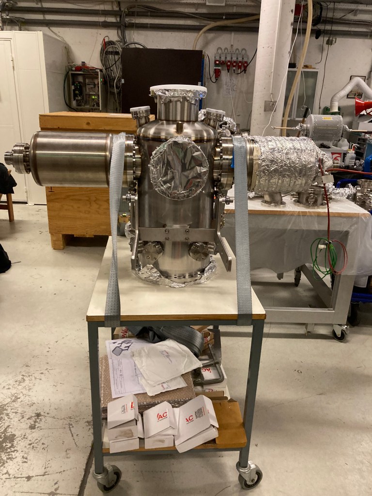
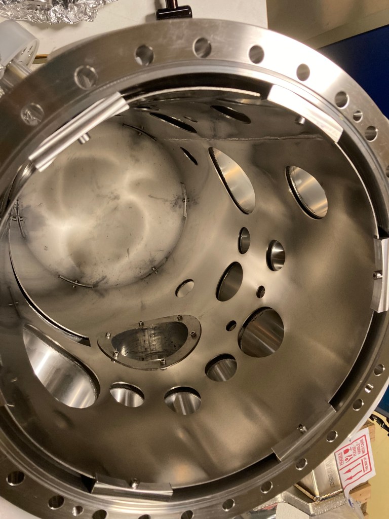
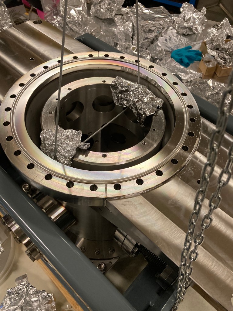
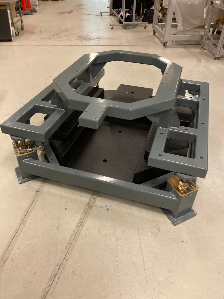
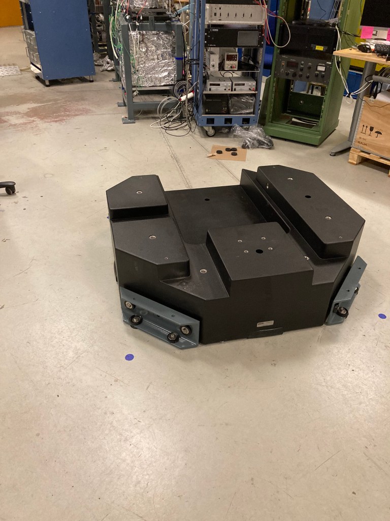
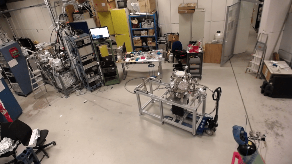
The videos and images below present milestones and timelapse photography for the beamline and end-station construction process.
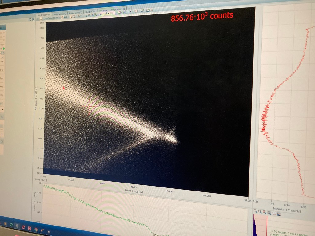


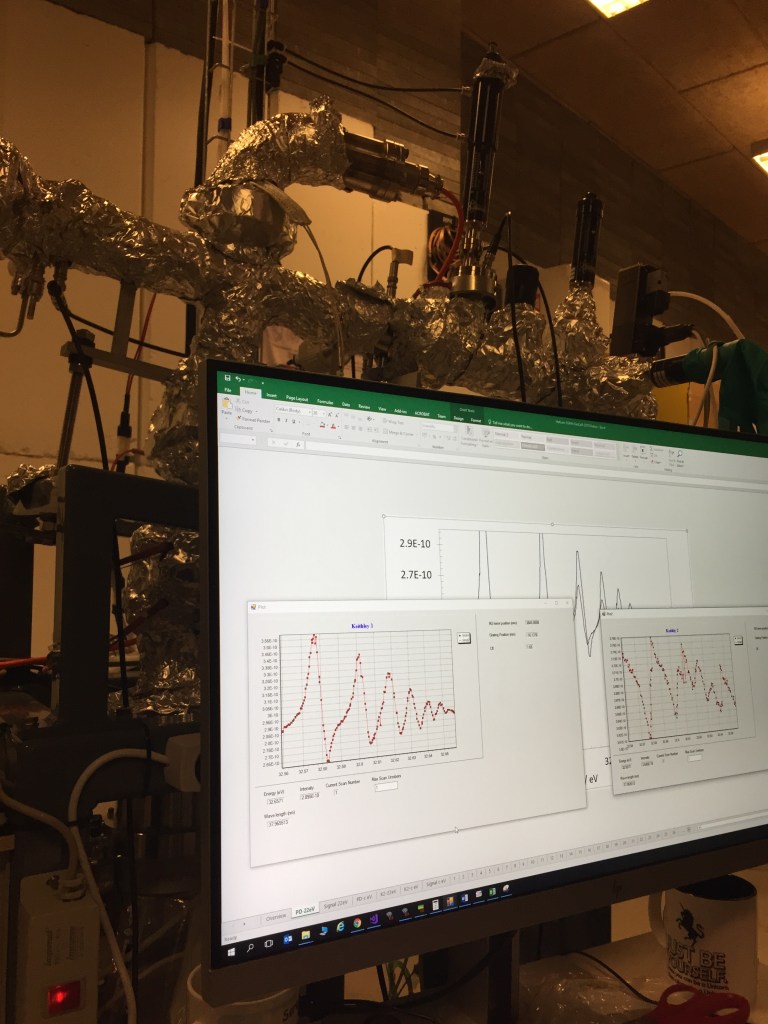
First measurements with our SPECS Phoibos 150 SAL, demonstrating the deflection capability of several lens modes. Here, scans are shown of bilayer graphene on silicon carbide around the corner of the Brillouin zone: